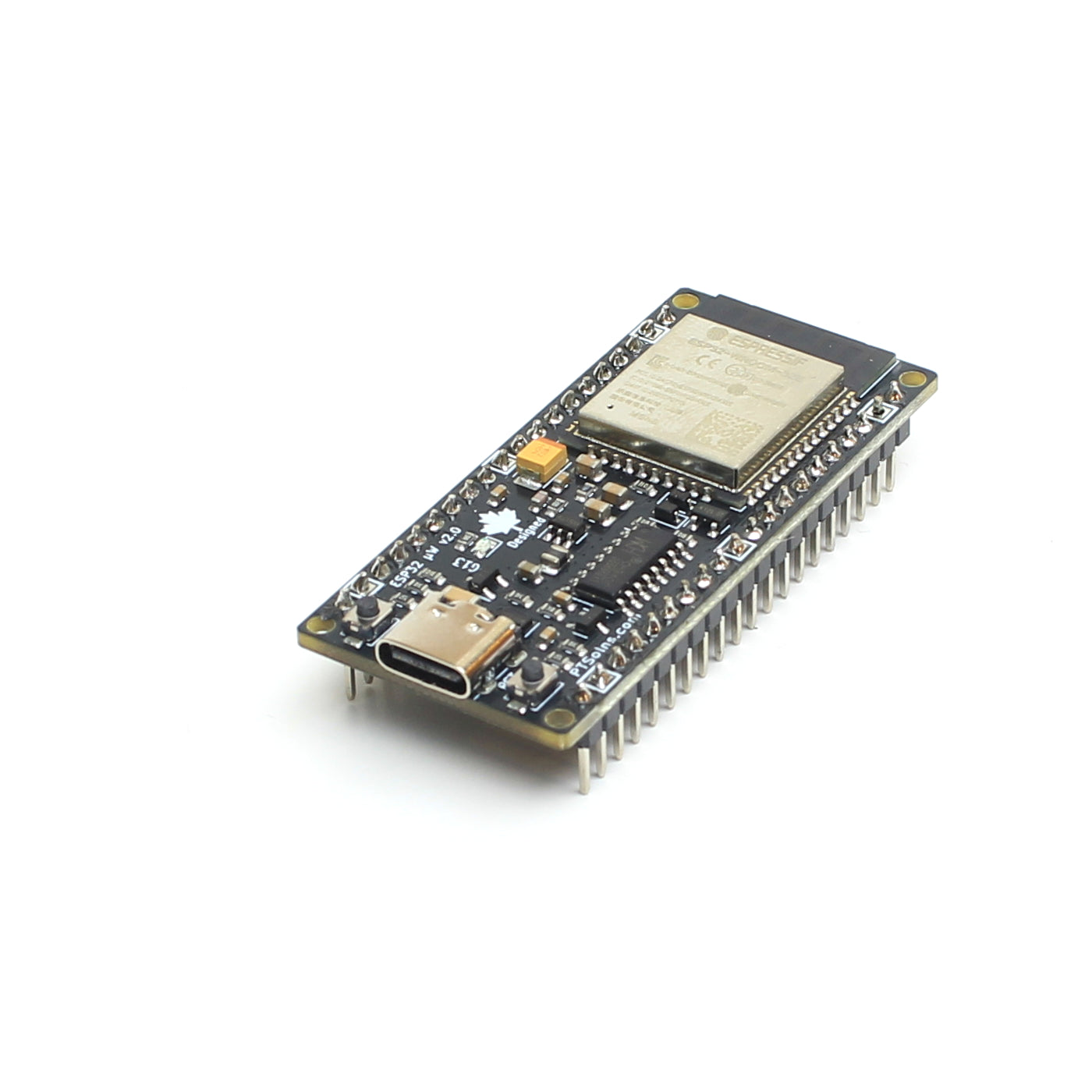

Every hardware project starts the same way: a desk covered in jumper wires, a breadboard that barely holds together, and a circuit that only works if you hold it at a very specific angle. We’ve all been there. It’s the messy, chaotic birth of a great idea.
But eventually, you have to move past the prototype. Whether you are building a smart home IoT gateway, a custom sensor node, or looking to commercialize a new piece of hardware, you need a system that is robust, reliable, and repeatable.
Here is the workflow for taking your project out of wiring hell and turning it into a professional, production ready custom PCB.

1. The Prototype Phase: Proving the Concept
Before you even think about firing up your PCB layout software, you need a rock-solid proof of concept. If your baseline circuit is flawed, your final board will be too.
The goal here is embedded circuit validation. Skip the flimsy components and lock down your logic using secure breakout platforms like a solid Raspberry Pi Pico Base or robust microcontrollers like the PTSolns Nano Flip. Building on a stable foundation allows you to test your code, verify your I2C communications, and ensure your power draw is exactly what you expect before committing to a digital design.
2. Schematic Capture & Multi-Layer Routing
Once your physical prototype is working perfectly, it is time to move to the digital realm. This phase is all about schematic capture and translating your physical wires into a logical diagram using industry standard EDA tools like KiCad, Altium Designer or EasyEDA.
Here is where the real engineering happens:
- Custom Component Footprints: Don't settle for "close enough." If your specific module or switch isn't in the standard library, take the time to build a custom footprint. It saves massive headaches later.
- Multi Layer Routing: When moving to the actual PCB layout, proper routing is critical. Keep your high speed data lines short, isolate your analog signals from noisy digital traces, and make good use of ground pours.
- Trace Widths: Make sure your traces can handle the current you are pushing. If you aren't sure how wide to make them, check out our PCB Trace Width Calculator (TTB #13) to get the exact numbers you need.
3. Manufacturing: Getting the Files Ready
You have a beautiful layout on your screen. Now you need to turn it into physical fiberglass and copper.
The handoff between your EDA software and the fabrication house relies on generating flawless Gerber manufacturing files. These files tell the manufacturer exactly where to drill holes, lay copper, and apply the solder mask.
Before you zip up those files and send them off to a fab house like JLCPCB, do a final design rule check (DRC). Pay special attention to your PCB silkscreen layout. Make sure your pinout labels, logos, and component designators are aligned, readable, and not sitting over bare copper or drill holes.
4. The Final Polish: Enclosures and Real World Testing
A bare circuit board is a beautiful thing, but a professional product needs a professional housing.
This is where parametric modeling comes in. Using software like Autodesk Fusion 360 allows you to design a custom enclosure perfectly dimensioned to your new board's mounting holes and port layouts.
For the initial physical tests, functional 3D printing is your best friend. Fire up your FDM printer like an Anycubic Vyper or Kobra and run off a prototype. While standard PLA is great for quick test fits, you will likely want to print the final functional enclosures in PETG. It offers the temperature resistance and structural durability needed to protect electronic hardware in the real world. Want to see what's possible with custom 3d Printed enclosures and jigs? Take a look at this video produced by the PTSolns team.
Bring Your Hardware to Life
Taking a project from a breadboard to a manufactured custom board is one of the most satisfying processes in electronics. It takes patience, careful routing, and a lot of double-checking, but the result is a clean, professional piece of hardware you can actually deploy.
If you are just starting your prototyping journey, check out the PTSolns Store for the development boards and modules you need to get off the ground.
Running into roadblocks scaling up? We don't just sell the hardware; we build it. Reach out to the team at PTSolns for custom electronic hardware engineering services, and let's get your idea ready for production.