
In this technical post, we explore the widely used CH340 IC from WCH, a popular USB-to-serial converter. The CH340 enables USB communication by translating USB signals to standard UART (serial) communication. It's commonly used to add serial ports to microcontrollers or legacy devices—making it ideal for programming, debugging, and data transfer applications.
While there are many ICs that serve a similar purpose, the CH340 stands out among makers and hobbyists for its affordability and ease of use. Compared to more expensive alternatives like the FTDI chip, the CH340 is significantly more cost-effective. Typically, it only requires a one-time driver installation, which we've covered in our video: Installing the CH340 Driver.
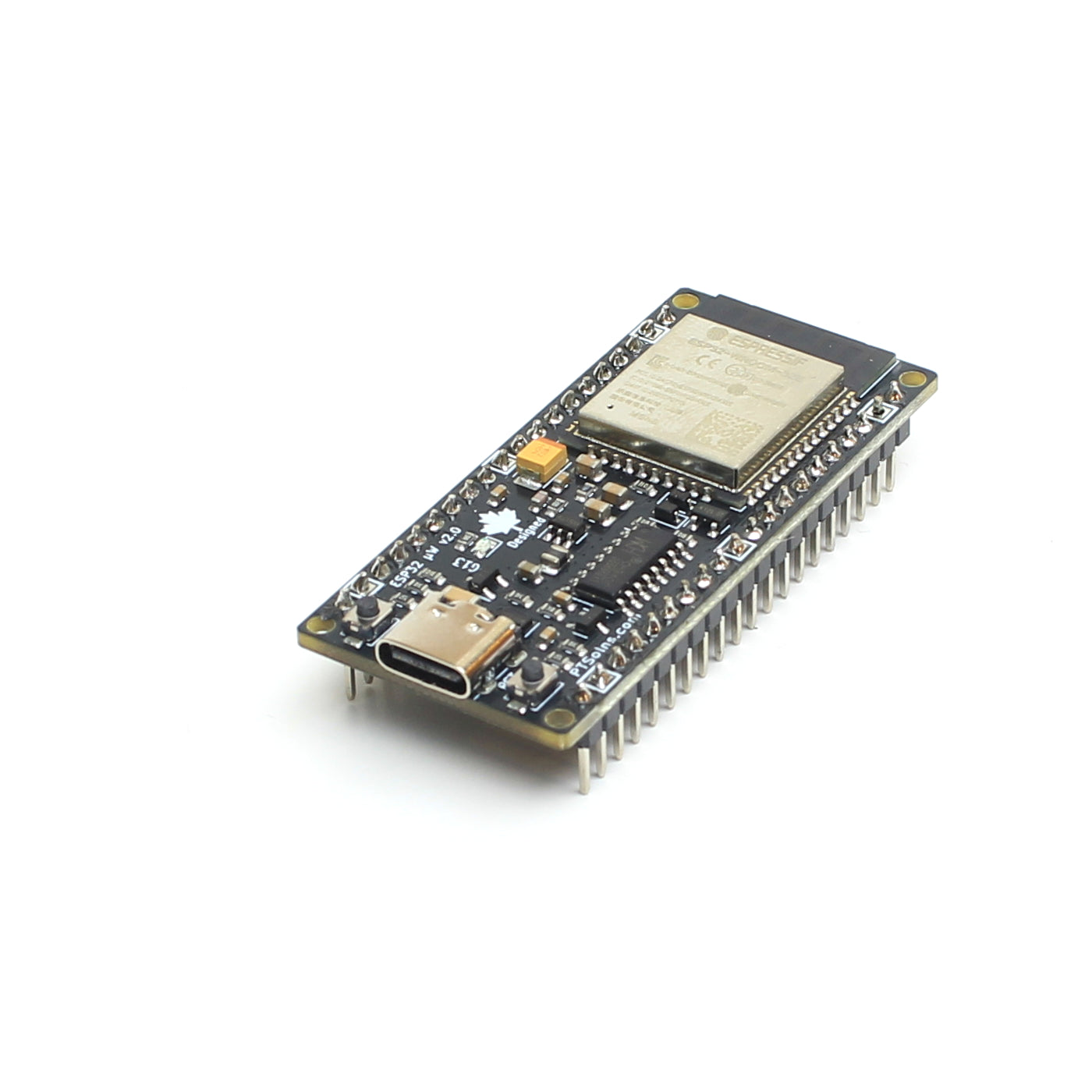
We're strong advocates of this IC and have integrated it into several of our products, including the Nano Flip, Uno R3+, and ESP32 microWatt. In all these designs, the CH340 functions in the same way—connecting the USB-C differential data lines (D+ and D−) to the microcontroller’s TX and RX pins. This enables simple and reliable USB programming.

In our designs, we specifically use the CH340C, which includes an internal 12MHz crystal, simplifying the layout and BOM. Another common variant is the CH340G, which requires an external 12MHz crystal. SparkFun Electronics is known to use this version, and it performs just as well in similar applications.
We're currently developing a new product that also integrates the CH340C USB-to-serial converter. While working on the schematic of our new product, we stumbled upon something curious—an unconventional use of the CH340 in one of SparkFun's published schematics.
Specifically, SparkFun’s implementation appears to violate the official not-so-detailed WCH CH340 datasheet. Intrigued, we dug deeper and ran a series of bench tests to understand how their configuration still works reliably. After some experimentation, we believe we've uncovered the reasoning behind their design—and how it manages to operate the CH340 without issues despite the apparent deviation from spec.
So, what exactly is this datasheet violation, and why does it still work? Let’s break it down!
The CH340 V3 Pin Violation
The discussion is all around the V3 pin (which is treated the same for the CH340C and the CH340G). In the latest version v3.4, which appears to have been updated on March 12, 2025, the official WCH CH340 datasheet has specific instructions on how to connect this pin. On page 5 in section 5.1 it states:
The CH340 chip supports 5V power supply voltage or 3.3V power supply voltage. When using a 5V operating voltage, the VCC pin of the CH340 chip inputs an external 5V power supply, and the V3 pin should be connected to an external power supply decoupling capacitor with a capacity of 0.1uF. When using a 3.3V working voltage, the V3 pin of the CH340 chip should be connected to the VCC pin, and an external 3.3V power supply should be input at the same time, and the working voltage of other circuits connected to the CH340 chip should not exceed 3.3V.
There are other similar notes such as in the table of Section 4:
When the power supply voltage is 3.3V, connect VCC to input the external power supply. When the power supply voltage is 5V, connect an external decoupling capacitor with a capacity of 0.1uF.
And even in the tables outlining the electrical characteristics of the IC (see Tables 6.2 and 6.3). It seems clear that WCH specifies the V3 pin two have two different configurations when powering the CH340 with VCC=5V or VCC=3.3V. The image below shows these two modes of configuration (not considering any other pin connections besides V3 and VCC).
- 5V configuration mode (image on the left): V3 pin connected to a capacitor and VCC=5V
- 3.3V configuration mode (image on the right): V3 pin connected to VCC=3.3V

This seems all good and clear. Now here's the crux. Let's take a look at SparkFun's schematic of their Basic Serial Breakout (a very useful product, BTW). This component has a solder jumper pad that can select VCC of the board to be either 3.3V (default) or 5V. With this jumper selection this board can be used to program both 3.3V logic level microcontroller development boards (such as the 3.3V Pro Mini) and 5V logic level microcontroller development boards (such as the 5V Pro Mini). Great!
Now here it is... in their schematic, which is publicly available to download, they show the V3 pin is hardwired to the capacitor (the 5V configuration mode). Below is a screenshot of their schematic showing this. Note that they use a different PCB design software than us, so their symbols look a bit different, including the pin arrangement. But what is important here is only the V3 pin.

Why the CH340 V3 Pin Violation is not a Problem
Obviously the V3 pin violation is not so serious, and SparkFun's product works as intended while the CH340 remains reliable. So what's going on? We had hinted earlier at the WCH datasheet being not so detailed, one of the reasons we did that is because there are no published documents or schematic on the inner workings of the CH340. Now they are not obligated to publish this, but it would help in our analysis. In any case, the most important part is what's happening internally between the VCC pin and the V3 pin.
We reckon that there is an internal Low Dropout Regulator (LDO) with the input being pin VCC and the output pin being V3. V3 is not just an output, however, it is also supplies other functions internally. This makes sense as the datasheet says to put a decoupling capacitor on V3 when VCC=5V as it is required for the LDO to remain stable. When VCC=3.3V, there is not enough voltage headroom for the LDO to provide 3.3V and so the datasheet says to bridge VCC to V3, effectively by-passing the LDO entirely.
When VCC=3.3V, the LDO is in dropout mode. In dropout mode, the CH340’s internal 3.3V regulator can no longer maintain a regulated output because the input voltage (VCC = 3.3V) is equal to or only slightly above the target output. When this happens, the regulator’s pass transistor fully saturates (i.e., turns on hard), allowing the input voltage to pass through to the V3 output with only a minimal voltage drop — typically just the transistor’s saturation voltage, which is usually in the range of a few tens of millivolts. This means V3 will sit just below VCC, still high enough to power the chip’s internal 3.3V domain reliably.
This is of course only true when the current draw on the V3 pin (with VCC=3.3V) is very low. We've done some measurements and found that when VCC=5V, the CH340C draws around 5.4mA with nothing else connected. In contrast, when VCC=3.3V, the CH340C only draws around 3.2mA. However, the V3 pin could also be used to power an external load, and not just supply the internal needs. It is unclear exactly what the current ratings of the LDO used inside the CH340 are (another reason why the WCH datasheet is not-so-detailed), however, from testing and scanning through community comments, we reckon one can draw around 20-30mA from the V3 pin.
This is the very crux of it all. In SparkFun's board, they are not drawing any current from the V3 pin to power an external load. Therefore, the voltage on the V3 pin remains close to VCC=3.3V, even though the V3 pin is not connected to the VCC (the V3 pin violation). Therefore, the CH340 continues to operate reliable.
We've done some tests on this and wanted to find out exactly what happens if an external load does draw a current from the V3 pin. The table below our results.
| Test | VCC | Rload | V3 Measured |
| Test 1 | 5V | Off | 3.26V |
| Test 2 | 3.3V | Off | 3.25V |
| Test 3 | 5V | ~28mA draw | 3.25V |
| Test 4 | 3.3V | ~28mA draw | 2.90V |
In Test 1, which is officially supported in the WCH datasheet, we see that the LDO regulates the V3 voltage to 3.26V (we measured a small peak-to-peak ripple for all tests of about 24mAV). Similarly, Test 3 also provides expected results - although we don't really know what the current ratings of the LDO are, we see that drawing 28mA with VCC=5V is stable.
In Test 2, which is in violation of the WCH datasheet, we see that still V3 remains close to the VCC, although V3 and VCC are not connected in SparkFun's design. Because V3 remains close to VCC=3.3V the CH340 continues to operate reliably. SparkFun must have also figured this out, as we are now, and implemented this in their design. Brilliant!
Finally, in Test 4 we see how things can fail. When VCC=3.3V and an external load draw current, the LDO starts to give up and V3 voltage drops. In our test, drawing 28mA dropped V3 to 2.90V, which may or may not operate the CH340 reliably. Drawing even more current would surely and quickly drop the V3 voltage to unreliable and insufficient levels.
Wrapping it all Up
So there you have it. The conclusion is that as long as the V3 pin is not used to power any external load, it is likely OK to violate the WCH datasheet and hardwire the V3 pin to a capacitor for both the 5V configuration and the 3.3V configuration. As soon as a current is drawn on V3 with VCC=3.3V and the V3 pin is not connected to VCC as per the WCH datasheet instructions, then the V3 voltage starts to drop to unreliable levels.
Now you might wonder, is the V3 pin ever used by anyone to power external loads. Well, yes, some products do that. For example, common Chinese clones of the Ardunio Nano, such as the one pictures below does exactly that. But in this case it is ok as the Nano clone operates in the 5V configuration, which we saw in Test 3 supports a current draw of at least 28mA.

Note that our Nano Flip does not pass the V3 pin of the CH340 to the external 3.3V pinout. Instead, the Nano Flip has a dedicated LDO to supply the external 3.3V loads.
One final note here. What could an engineer or designer do to remain compliant with the WCH datasheet, but still offer the same voltage flexibility of toggling between 5V and 3.3V, as is done in SparkFun's board? A logic level shifter (LLS) would have to be implemented and the CH340 hardwired to the 5V configuration (in compliance). If the jumper is set on 3.3V, the LLS would drop the 5V signals (Tx, Rx, etc) to 3.3V. If the jumper is set on 5V, the LLS would pass through the 5V signals without the need to shift the logic. Food for thought, but not required in the design cases outlined in this blog.
With all this out of the way and done with, we can continue our product development of a new upcoming board (more detail on that in some time). And yes, for those of you who are thinking this, we will be implementing the V3 pin violation as well 😉